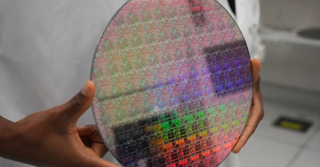
The Biden administration said on Tuesday that it would direct up to $1.6 billion in funding toward developing new technology for packaging computer chips, a major thrust in U.S. efforts to stay ahead of China in creating components needed for applications like artificial intelligence.
The proposed funding, part of the money authorized under the 2022 legislation called the CHIPS Act, will help companies innovate in areas such as creating faster ways to transfer data between chips in a package and managing the heat they generate, said Laurie Locascio, an under secretary in the Commerce Department who is also the director of its National Institute of Standards and Technology.
Her announcement, at an annual industry conference in San Francisco, serves as a starting gun for companies to start applying for grants to fund research and development projects, with awards expected to total up to $150 million each.
“Our research and development efforts in advanced packaging will heavily focus on high-demand applications like high-performance computing and low-power electronics, both needed to enable leadership in A.I.,” Ms. Locascio said.
The CHIPS Act received bipartisan approval to invest $52 billion to stoke domestic chip production, with most of the money directed toward the factories that turn silicon wafers into chips. The U.S. share of that activity has dwindled to around 10 percent, much of it lost to companies in Asia. U.S. reliance on factories run by Taiwan Semiconductor Manufacturing Company, or T.S.M.C., in particular, have worried policymakers because of China’s territorial claims on Taiwan.
The dependence on foreign companies is even more stark in chip packaging. That process attaches finished chips — useless without ways to communicate with other pieces of hardware — onto a flat component called a substrate, which has electrical connectors. The combination is typically wrapped in plastic.
Packaging mainly takes place in Taiwan, Malaysia, South Korea, the Philippines, Vietnam and China. A U.S. industry group called IPC, citing Defense Department data, has estimated that the U.S. only accounts for about 3 percent of advanced chip packaging.
With most federal funding so far directed toward the early stage of manufacturing, chips produced in new U.S. factories might then be flown to Asia for packaging, which would do little to reduce dependence on foreign companies.
“You can make all the silicon you want here, but if you don’t take it to the next step, it doesn’t do any good,” said Jan Vardaman, president of TechSearch International, a consultancy focusing on chip packaging.
The situation is being compounded by companies increasingly striving for greater computing performance by packaging multiple chips side by side or on top of each other. Nvidia, which dominates sales of chips for A.I., recently announced a product called Blackwell that has two big processor chips surrounded by stacks of memory chips.
T.S.M.C., which fabricates the latest chips for Nvidia, also packages them with advanced technology. T.S.M.C. is slated to receive federal grants for chip production in Arizona, but it hasn’t said it will shift any packaging services from Taiwan.
Intel, a Silicon Valley chip maker, is considered a leader in packaging research and has invested heavily to upgrade factories in New Mexico and Arizona as part of broader efforts to compete with T.S.M.C. in manufacturing services. But U.S. companies could use federal money to help stay on the cutting edge, Ms. Vardaman said.
The new grants are part of a plan called the National Advanced Packaging Manufacturing Program, which Commerce Department officials said would receive about $3 billion in total funding.
“Today’s announcement is another important step in the right direction,” said Chris Mitchell, IPC vice president of global government relations.
Some industry players aren’t waiting for government help. Resonac, a company based in Tokyo, announced on Monday a new consortium with nine other Japanese and U.S. companies to focus on packaging research and development in a new facility that will be built in Union City, Calif.
In an interview, Ms. Locascio of the Commerce Department said the administration this week would also announce its conceptual model for the National Semiconductor Technology Center, a proposed public-private partnership for chip research and development that is expected to include new facilities, which officials in multiple states hope to attract.
“We get a lot of calls daily about that,” Ms. Locascio said, adding that the announcement should clarify what kinds of facilities are envisioned and “the process by which people can compete for those.”


